Electrical Engineering ⇒ Topic : N-channel JFET
|
|
| Sachin
| |
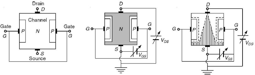
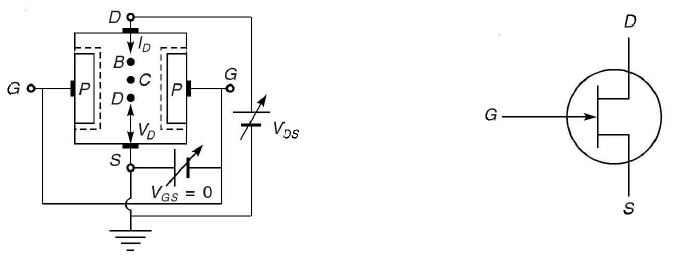
N-channel JFET The N-channel JFET is shown in Figure (a) by block representation. The piece of N-type material is known as the channel that has two terminals called source and drain. Two P-type materials are attached to the sides of the channel that form the P-N-junction. The two pieces of P-type materials are connected together. Their terminal is called gate. In Figure 1(a), the gate terminals are not connected and a potential is applied between drain and source (positive at drain and negative at source). The drain current ID flows. When gate is biased negative with respect to the source, the P-N junctions are reverse biased. The depletion region is formed as shown in Figure 1(b). The channel is generally lightly doped than P-type gate blocks. This helps the depletion regions to penetrate deeply into the channel. The depletion region behaves as an insulator because it is a region of depleted charge carriers. This tantamounts to narrow the channel and increase the resistance and ID is reduced. If the negative gate bias voltage is further increased, the depletion region in the channel penetrates deep near the drain (D) region due to the electric field at the reverse biased gate-channel junctions. So the name field effect transistor comes into play. Figure 1(c) shows the depletion region for large negative gate source bias (a) No bias voltage on gates (b) Small negative gate-source bias (c) Large negative gate-source bias figure (1) The N-channel JFET The drain current causes a voltage drop along the channel because the N-material is resistive. The flow of ID in the channel causes a voltage drop that biases the gate with respect to that part of the channel close to the gate. In Figure (2), point B is positive w.r.t. the source and in other words, the source terminal voltage is negative w.r.t. the point B. The gate regions are connected to the source. Therefore, the gate regions are negative w.r.t. the point B by voltage VB.This causes the depletion region to penetrate into the channel at point B by an amount proportional to VB. Similarly, for points C and D, the penetration of depletion region is less ascompared to B because VD < VC< VB. This is shown in Figure (2). The symbol for N-channel is represented in Figure (3). Figure (2) Formation of depletion region. Figure (3) Symbol for N-channel JFET. | |
|
| |
!! OOPS Login [Click here] is required for more results / answer